



Empilement Hybride Haute Fréquence : Ingénierie d'une carte à 8 couches avec RO4350B, FR-4 et laminage séquentiel
ContPerson : Sally Mao
Numéro de téléphone : 86-755-27374847
Je suis désolé. : +8618277967574
| Quantité de commande min : | 1 pièces | Prix : | 0.99USD/PCS |
|---|---|---|---|
| Détails d'emballage : | emballage | Délai de livraison : | 2-10 jours ouvrables |
| Conditions de paiement : | T/T, Paypal | Capacité d'approvisionnement : | 50000 pièces |
| Lieu d'origine: | Chine | Nom de marque: | Panasonic |
|---|---|---|---|
| Certification: | ISO9001 | Numéro de modèle: | M6 |
Description de produit
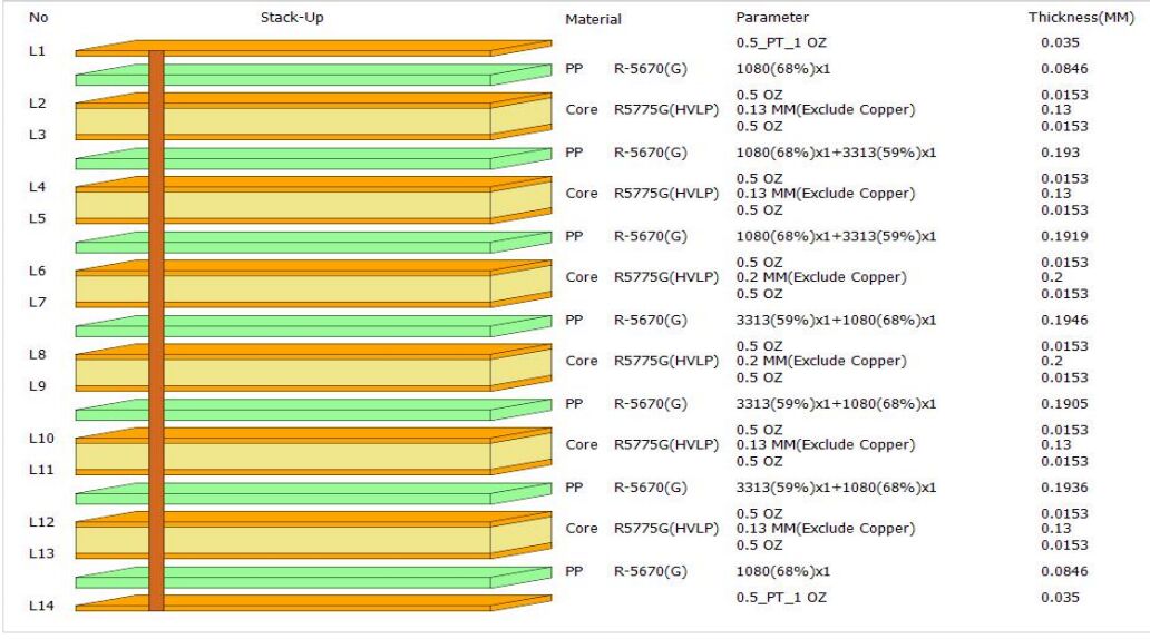
Un PCB M6 à 14 couches avec contrôle d'impédance multipoint
Au fur et à mesure que les débits de données dépassent 25 Gbps et atteignent le domaine de 56G et 112G PAM4, les matériaux de PCB conventionnels comme le standard FR-4 atteignent leurs limites pratiques.et le choix du matériau stratifié détermine directement si une conception à grande vitesse réussit ou échoueCet article examine une carte sophistiquée de 14 couches construite sur le matériau M6, avec un contrôle d'impédance rigoureux à cinq points critiques, fiabilité de classe IPC-3,et avancés par des techniques de transformation.
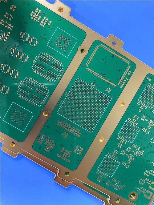
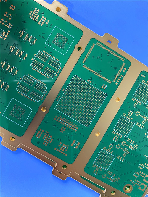
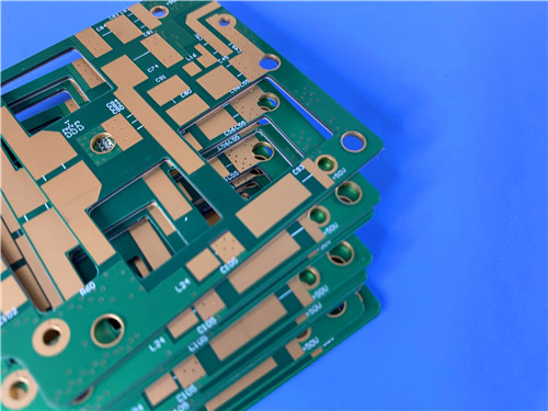
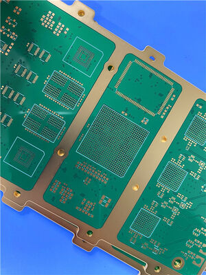
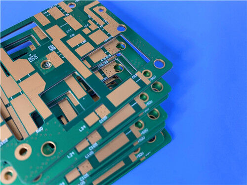
Capture d'écran du produit: La carte haute vitesse à 14 couches
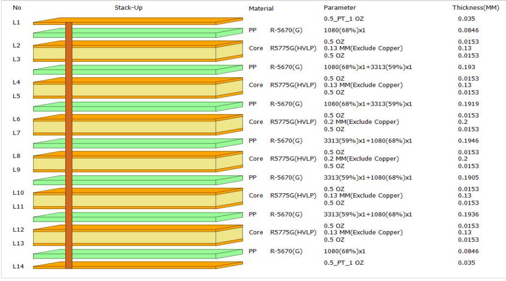
Nombre de couches: 14 couches
Matériau de base: série M6 (laminé R-5775 ((N), prépreg R-5670 ((N))
Épaisseur du panneau fini: 2,406 mm
Poids du cuivre: couches intérieures 0,5 once de cuivre fini, couches extérieures 1 once de cuivre fini
Masque de soudure: vert avec lettres blanches
Finition de surface: nickel-palladium-or (ENEPIG)
Taille du panneau: 106 mm x 102 mm = 1 pièce
Norme de qualité: classe IPC-3 (haute fiabilité)
Contrôle de l'impédance: 5 paires de différentiels, chacune réglée à 100Ω ± 10%
Vias: de 0,2 mm de diamètre, bouchées en résine, galvanisées pour lisser la surface
Qu'est-ce que le matériau de la carte M6?
Le M6 est un matériau stratifié à haute vitesse et à faible perte de la série Megtron, spécialement conçu pour les applications nécessitant une intégrité supérieure du signal à haute fréquence.
Les deux sont classés comme "Matériaux multicouches à haute vitesse et à faible perte" avec une construction en tissu en verre à faible Dk, ce qui réduit le retard de propagation du signal et améliore la cohérence de l'impédance.
Tableau des paramètres clés (à partir de la fiche R-5775 ((N))
| Les biens immobiliers | Condition d'essai | Valeur typique |
| Température de transition du verre (Tg) DSC | Comme reçu | 185°C |
| Température de transition du verre (Tg) DMA | Comme reçu | 210°C |
| Température de décomposition thermique (Td) | TGA | 410°C |
| Il est temps de Delam (T288) | Je ne sais pas. | > 120 min |
| Il est temps de Delam (T288) avec Cu | Je ne sais pas. | > 120 min |
| Le système d'échantillonnage doit être utilisé pour les essais d'échantillonnage. | < Tg | 45 ppm/°C |
| Constante diélectrique (Dk) | C-24/23/50 Le gouvernement fédéral | 3.4 |
| Constante diélectrique (Dk) | Nombre d'équipements | 3.34 |
| Facteur de dissipation (Df) @ 1 GHz | IPC 2.5.5.9 | 0.002 |
| Facteur de dissipation (Df) @13GHz | Nombre d'équipements | 0.0037 |
| Résistance au volume | C-96/35/90 Le gouvernement fédéral | 1 × 10⁹ MΩ·cm |
| Résistance de surface | C-96/35/90 Le gouvernement fédéral | 1 × 10⁸ MΩ |
| Absorption de l'eau | D-24/23 | 00,14% |
| Résistance à l'écaillage (1 once de feuille H-VLP) | Comme reçu | 00,8 kN/m |
| Intégrabilité | Leur valeur | V-0 |
M6 Variantes de matériau (types de noyau)
Le M6 est disponible en plusieurs épaisseurs de noyau, chacune avec des styles de tissu de verre spécifiques et une teneur en résine:
| Type de noyau | Épaisseur réelle (mm) | Style du tissu en verre | Contenu en résine (%) | Dk @ 1 GHz | Df @ 1 GHz |
| Type 2 | 0.05 | 1035 | 67 | 3.25 | 0.002 |
| Type 4 | 0.1 | 2013 | 56 | 3.4 | 0.002 |
| Le type 5 | 0.125 | 2116 | 56 | 3.4 | 0.002 |
| Type 8 | 0.2 | 2013 | 56 | 3.4 | 0.002 |
| Le type 10 | 0.25 | 2116 | 56 | 3.4 | 0.002 |
| Le type 30 | 0.75 | 2116 | 56 | 3.4 | 0.002 |
Domaines d'application du M6
L'informatique haute performance (serveurs, commutateurs, routeurs)
Transcepteurs optiques (400G, 800G)
Infrastructure de télécommunications (stations de base 5G, liaisons rapides)
Équipement d'essai et de mesure
Aérospatiale et défense (radar, guerre électronique)
Points de traitement clés pour le M6
Sur la base de la ligne directrice M6, les fabricants doivent prêter attention aux éléments suivants:
Conservation: le Prepreg R-5670 doit être conservé à ≤ 23°C et ≤ 50% RH. Un stockage prolongé nécessite une température de 5°C. Les sacs ouverts doivent être recouverts; l' exposition cumulée ne doit pas dépasser 8 heures.
Traitement par liaison à la couche interne: l'oxyde noir/brun est acceptable, mais un traitement par oxyde alternatif (technologie de gravure au peroxyde/sulfure) est préférable.Il est recommandé de cuire à 105 °C pendant 20 à 30 minutes après traitement à l'oxyde..
Perçage: utilisez des trous à angle d'hélice élevé et des feuilles d'entrée lubrifiées (par exemple, des feuilles LE).charge de la puce de 20 μm/rev3000 visites.
Pour le déshumidificateur de permanganate, le temps de déshumidification FR-4 est deux fois plus long que pour le déshumidificateur de plasma, la moitié du temps de déshumidification FR-4.Pour les constructions hybrides avec FR-4, un traitement combiné (découpage plasma + permanganate sans gonflement) est recommandé.
ENIG Précautions: si vous utilisez ENIG (comme ce produit), cuire à 150°C pendant 5 heures ou conserver à température ambiante pendant 1 semaine est nécessaire avant le nickelage afin d' éviter les défauts du placage.
Lamination: Vitesse de chauffage: 2,0 à 4,0°C/min. Pression: 3,0 à 4,0 MPa. La température du produit doit dépasser 185°C pendant 75 minutes. Arrêt sous vide à 90 à 130°C (30 minutes après le démarrage).
Types d'impédance
Le contrôle d'impédance est la pratique consistant à faire correspondre l'impédance caractéristique d'une ligne de transmission à l'impédance de source et de charge pour minimiser les réflexions du signal.cinq paires de différentiels sont réglées à 100Ω ± 10%Examinons les principaux types d'impédance et leur application.
Impédance à extrémité unique
Un seul conducteur référencé à un plan terrestre (généralement sur une couche adjacente).
Impédance différentielle
C'est le type utilisé dans le produit courant. Deux traces correspondantes transportant des signaux égaux et opposés. L'impédance différentielle est l'impédance entre les deux traces.La valeur standard pour les paires différentielles à grande vitesse (USB), PCIe, Ethernet, LVDS) est de 100Ω.
Pourquoi un différentiel de 100 Ω?Cette valeur équilibre la consommation d'énergie, l'immunité au bruit et la compatibilité avec les conceptions d'émetteurs-récepteurs standard.
Impédance coplanaire
Les traces sont référencées sur les plans au sol de la même couche (via des déversements au sol adjacents) en plus d'un plan de référence en dessous.souvent utilisé dans les conceptions RF ou lorsque l'espacement de couche en couche est incohérent.
Microstrip contre Stripline
| La structure | Définition | Les avantages | Les défauts |
| Microstrip | Trace de la couche extérieure avec un seul plan de référence en dessous | Plus facile à fabriquer, moins de pertes, accessible à la sonde | Plus sensible au bruit croisé et à l'EMI |
| Ligne à rayures | Trace de la couche interne avec les plans de référence au-dessus ET en dessous | Excellent blindage contre les émissions électromagnétiques, champ symétrique, impédance constante | Perte plus élevée, plus difficile à fabriquer, propagation plus lente |
Structures d'impédance dans ce produit
À partir de la feuille de calcul de l'impédance, nous pouvons identifier deux structures distinctes:
1. Microstrip recouvert par couplage de bord 1B (impédance 1 et 2 L1 et L14)
2L'impédance de l'écoulement de la ligne 1B1A (impédance 3, 4, 5 ¢ L5, L10, L12)
Pourquoi cinq points de contrôle d'impédance?
Les cinq paires de différentiels contrôlés (L1, L14, L5, L10, L12) reflètent la complexité du routage à grande vitesse:
L1 et L14 (couches extérieures): vraisemblablement pour les signaux qui doivent entrer/sortir de la carte sans voies, ou pour les points d'essai.
L5, L10, L12 (couches intérieures): structures de lignes de ligne pour les traces longues et à grande vitesse nécessitant une protection EMI maximale et une impédance constante sur de plus longues distances.
La hauteur diélectrique (H1/H2) et la hauteur diélectrique (Er1/Er2) de chaque couche diffèrent en raison de l'empilement, ce qui nécessite des réglages indépendants de la largeur de trace (W) et de l'espacement (S) exactement comme indiqué dans les colonnes "Réglé".
Autres caractéristiques de fiabilité
Les principales exigences sont les suivantes:
Test électrique à 100% pour la continuité et l'isolation
Exigences plus strictes en matière d'anneaux annulaires (minimum 50% du tampon)
Qualité plus stricte des parois des trous (pas de vides, pas de fissures après stress thermique)
Remplissage complet des trous plaqués (pas de vides dans le cuivre)
0.2 mm Vias: Résine enroulée + lissage électroplaté
Les petites voies (0,2 mm de diamètre) sont standard pour les conceptions à haute densité.
Cependant, les voies ouvertes peuvent causer des problèmes:
Le soldeur est enlevé pendant l'assemblage
Flux piégé provoquant une dégazation
Surface inégale pour le placement des composants
Le collage en résine remplit complètement la voie avec une résine époxy non conductrice.
Cela permet:
Conception via-in-pad (via placés directement sous les plaquettes BGA)
Amélioration de la fiabilité (pas de vides, pas de contaminants piégés)
Meilleure dissipation de chaleur (couvercle en cuivre solide)
Conclusion
Ce circuit imprimé M6 à 14 couches représente l'état de l'art de la conception numérique à grande vitesse.Confiance de la classe IPC-3La carte est spécialement conçue pour les applications nécessitant une intégrité du signal à plus de 25 Gbps.
L'utilisation de structures à microstrip (L1, L14) et à stripline offset (L5, L10, L12) démontre une compréhension sophistiquée du contrôle d'impédance entre différents types de couches.Pour les ingénieurs spécifiant des cartes similaires, l'attention portée au stockage des matériaux, aux paramètres de forage, aux cycles de démaquillage et au précuisson ENIG (tel que détaillé dans les lignes directrices du procédé M6) est essentielle à la réussite du premier passage.
Entrez votre message

RO4350B, 4003C ; Rogers 5880, 5870, 6002, 6010, 6006, 6035 ; RO3003, RO3035, RO3006, RO3010, RO3210, RO3203
TLX-8, TLX-6, TLX-9, TLX-0, TLX-7, TLY-3, TLY-5, RF-35TC, RF-60TC, RF-35A2, RF-60A, AD450, AD600, TMM4, TC350
| Shenzhen Bicheng Electronics Technology Co., Ltd |
| ville de 6-11C Shidai Jingyuan Fuyong, secteur de Baoan, ville de Shenzhen, province du Guangdong, Chine |
| 86-755-27374946 |
| sales30@bichengpcb.com |